DIGITAL OUTPUTS
INTRODUCTION:
Digital outputs are the most basic (and often use) from of outputs. The AVR pin will send out a LOW (GND) or HIGH (Vcc) signal. It is important to note that the pin goes from 0V to Vcc and not from OFF to ON. The difference is not simply semantics because, hardware that turns devices OFF tends to provide a physical break in the wire stopping current flow (devices such as relays, switches, contactors), while a pin configured as a digital output will change from 0V to Vcc. This is important to keep in mind because it allows us to do some interesting things with our hardware design.
HARDWARE:
If you look at the AVR data sheet, the second page shows the pin configuration of the AVR chip. All the PA#, PB#, PC# and PD# could be configured as an outputs.
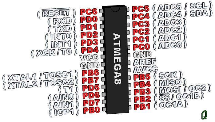
Figure 1: ATmega8 - Outputs
We can design a circuit in 2 ways, the pin can SINK the output (put it down to ground) or SOURCE the output (bring it up to Vcc). Confused? Well lets clear things up in the following 3 examples.
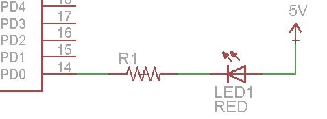
Figure 2: Sinking Output
In figure 2 we are sinking the output. Notice how the LED is hooked up to Vcc on one side and to the digital output pin on the other side. When the digital output is set to HIGH(Vcc) and the other side is at Vcc (say 5V) there is no potential difference ie 5V – 5V = 0 (no difference) so the LED will not light-up. However, if we set the digital output to LOW (GND or 0V) we have a 5V difference between the pin and the common side (0V – 5V = 5V difference) hence the LED will come on.
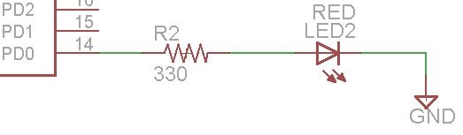
Figure 3: Sourcing Output
In figure 3 we are sourcing the output. One side of the LED is hooked up to the digital output and the other side is connected to ground. When the digital output is set to HIGH(Vcc) the LED will turn on (Because we have a 5V difference between the digital pin and the common of the LED). When we set the digital pin to LOW(GND) the LED will turn off because,the digital output pin is at 0V and the common side of the LED is at 0V which means we have no potential difference between both sides of the LED.
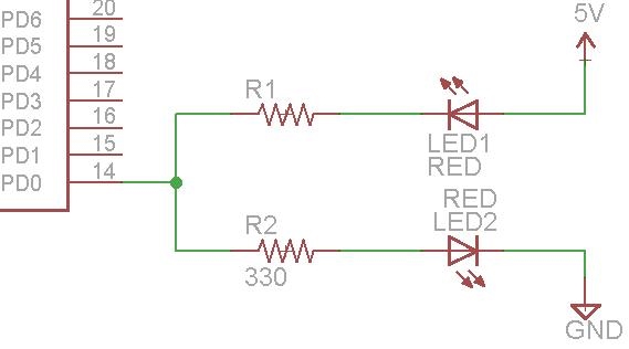
Figure 4: Sinking and Sourcing On The Same Output
Figure 4 is a neat little circuit we have 2 LEDs hooked up to the same digital output. LED 1 is hooked up for sinking (like in figure 2) , and LED 2 is hooked up for sourcing (like in figure 3). When we set the digital pin to LOW(GND or 0V) LED 1 will turn on and LED 2 will stay off, if we change the pin to HIGH(Vcc) LED 1 will stay off and LED 2 will turn on.
NOTE: LEDs are polarity specific which means that they have to be hooked in the right way in order to work, if you decide build any of these circuits, and you can’t get things to work, turn the LED around and try again.
So, you might wonder to yourself, which is preferred, sinking (figure 2) or sourcing (figure 3)? The answer is sinking, most electrical components have an easier time with sinking, some can even sink more current than they could source. So keep your eyes open for this in the future.
Maximum Output Capabilities:
This leads us to our final topic. Outputs on most AVR's are limited in how much current they can output. If you download the ATmega datasheet(link on side) the information is located in the “Electrical Characteristics” section. So lets take a look at the Electrical Characteristics (top of section) of the Atmega168/328 datasheet. Notice that under the "Absolute Maximum Ratings" it lists that the DC Current per I/O pin is 40mA’s. That’s pretty good since it means we can safely drive any LED with each pin (most LEDs run at 10-20mA). However, notice that the DC Current Vcc to GND Pins is 200mA, that is the absolute maximum that the processor can drive at once. So, whenever you design a circuit make sure you look at these 2 values, going beyond those values will result in damage to your microcontroller. So that seems fairly simple, make sure that every single load (or device your driving) does not exceed the Absolute Maximum Rating Per pin, and that every output added up does not exceed the Maximum DC from Vcc to GND, this is all that you have to look at if you're just playing around however, running your AVR at these values for prolonged periods of time will cause damage over time.
So if you look at the DC Characteristics Table you will notice that Ioh (voltage of output high) and Iol (voltage of output low) you will notice that each output is limited to 20mA @5V or 10mA @ 3.3V, the voltage is the voltage of Vcc (or the voltage that we are running our AVR at. So that is the Max per pin done, do we have a rule for Maximum DC from Vcc to GND? You bet we do. Look at the notes under the table, they list a lot of restrictions such as not exceeding 150mA if we add the values of the pins on C0-C5, D0-D4, ADC7 and the RESET pins. Although it seems like a pain, following these rules will keep your project running for a lifetime.
So I guess you wondering, what do I do if I want to run a load higher than 20mA? Well you will have to use an extra component between the microcontroller and the load. A transistor, FET or my personal favorite a Darlington Array will do the trick. But that is a chapter on its own.
THEORY OF OPERATION:
The one thing that I don't understand is why input/output section in the Atmega8 and Atmega328 is so poor. Every other part of the data sheet has a really nice description of each register at the end of each section that describes everything.
Under the I/O section of the data sheet you will find the following table:
| DDxn | PORTxn | PUD | I / O |
Pull-up |
Comments |
| 0 | 0 | x | input | No | Tri-state (Hi-Z) |
| 0 | 1 | 0 | input | Yes | Pxn will source
current if external pulled low. |
| 0 | 1 | 1 | input | No | Tri-state (Hi-Z) |
| 1 | 0 | x | output | No | Output Low (Sink) |
| 1 | 1 | x | output | No | Output High (Source) |
This table tells us everything we need to know, we just have to know how to read it. Since we are talking about outputs only the last 2 rows apply. What they state is that we have a common register that we have to set to 1 for output named DDxn (Data Direction Register), leaving the pin LOW(0) will make it an input but setting it to HIGH(1) will make it an output. Once DDxn is HIGH(1) we can set PORTxn to LOW(0) in order to provide us with a GND signal a.k.a. "output low (sink)". Or we could set it to HIGH(1) or provide us with a Vcc signal a.k.a. "Output High (Source)". The PUD(Pull Up Disable) register doesn't matter, so we are done.
The only mystery that remains is what's with the xn? "x" defines which Port we are using B, C or D (there is no A port on the ATmega328, but some like the Atmega32 do have them). The "n" defines the pin number. So this chart is telling us that if we want to make the PD0 pin an output we have to turn on DDD0 to HIGH(1) and after that when we change PORTD0 to a HIGH(1) we will output 5V and if we leave it LOW(0) we will get GND(or 0V).
We are almost done, there is just one thing left to do. We need to find what register where DDD0 and PORTD0 live in. So if you go to the "Register Summary" section, you can see that DDD0 is a bit within the DDRD register and the PORTD0 is a bit within the PORTD register.
NOTE: A lot of programmers will simply use 0-7 instead of PORTx0-PORTx7 and DDx0-DDx7, so don't be surprised if you see that if your going though peoples code.
SOFTWARE:
ATmega8 & ATmega168/328 Code:
    #include <avr/io.h>

    int main(void)
    {
        DDRD |= (1 << DDD0);        // sets bit DDD0 to 1 within register DDRD
        // PD0 is now an output WOOT !!!

        PORTD |= (1 << PORTD0);     // turn on PD0
        // PD0 is now an output and is sourcing VCC

        PORTD &= ~(1 << PORTD0);     // turn off PD0
        // PDO is still an output and is now sinking 0V

        while(1)
        {
            // main loop
        }
    }
Behold the mystery of the output revealed
Cheers
Q